IC Packaging Services and what they Entail
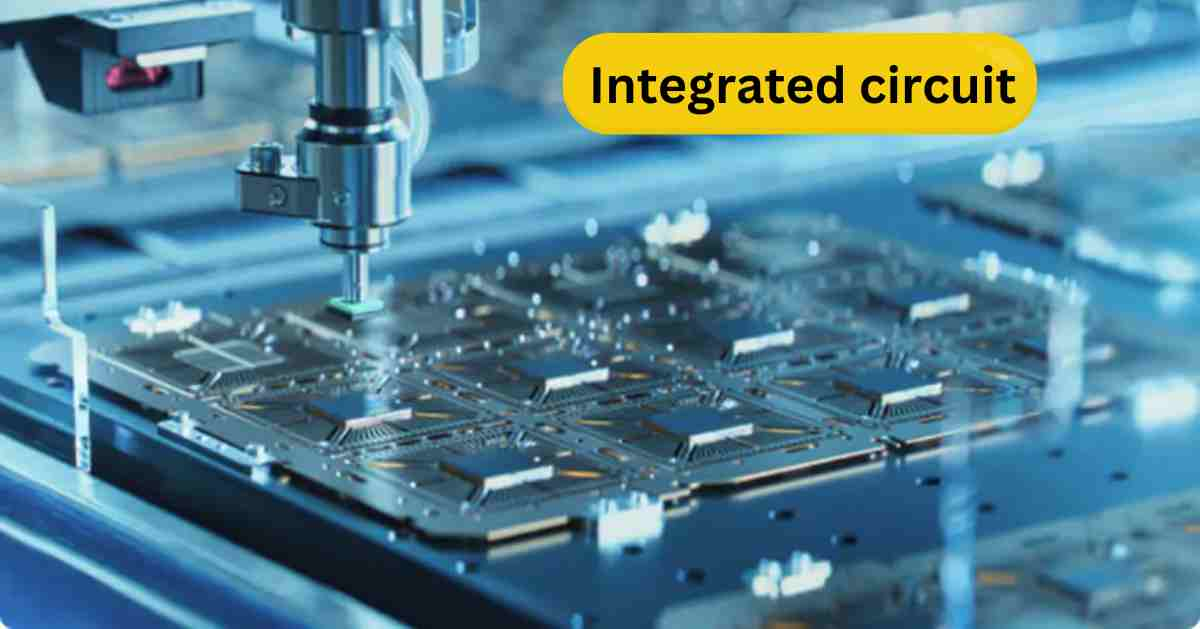
Integrated circuit or IC packaging is a critical step in the semiconductor manufacturing process, transforming a delicate silicon die into a robust and functional component ready for integration into electronic devices. This process involves encasing the die in a protective package, providing electrical connections, and facilitating heat dissipation. IC packaging services are diverse and tailored to meet the specific requirements of various applications, ranging from consumer electronics to high-performance computing.
The initial stage of IC packaging typically involves die preparation. This includes die attach, where the silicon die is securely bonded to a leadframe or substrate using an adhesive material. The leadframe provides a mechanical support and electrical pathways for connecting the die to external circuitry. Following die attach, wire bonding or flip-chip technology establishes electrical connections between the die’s contact pads and the leadframe or substrate. Wire bonding utilizes thin gold or copper wires to create these connections, while flip-chip technology involves directly soldering the die’s contact pads to the substrate, offering higher density and improved electrical performance.
[Read About: The Best Place to Buy Network Accessories for Quality and Value ]
Encapsulation is a crucial step in protecting the delicate silicon die from environmental factors like moisture, dust, and physical damage. This process involves molding a protective compound, typically epoxy molding compound (EMC), around the die and its connections. The encapsulation material provides mechanical strength and thermal stability, ensuring the long-term reliability of the packaged IC. Different encapsulation techniques, such as transfer molding and compression molding, are employed depending on the specific package type and application requirements.
After encapsulation, the packaged IC undergoes various finishing processes. This may include lead trimming and forming, where the leads are trimmed to the desired length and shaped for surface mounting or through-hole insertion. Surface finishing, such as tin plating or gold plating, is applied to the leads to enhance solderability and corrosion resistance. Marking and labeling are also performed to identify the packaged IC with relevant information, such as part number, manufacturer, and date code.
IC packaging services extend beyond the basic assembly processes to include advanced packaging techniques for high-performance applications. System-in-package (SiP) technology integrates multiple ICs and passive components into a single package, enabling higher levels of integration and miniaturization. 3D packaging, such as through-silicon vias (TSVs), stacks multiple dies vertically, further increasing density and performance. Fan-out wafer-level packaging (FOWLP) redistributes the die’s connections to a larger area, allowing for more I/O connections and improved thermal management.
Thermal PCB management is a critical consideration in IC packaging, especially for high-power devices. The packaging design must facilitate efficient heat dissipation to prevent overheating and ensure reliable operation. Techniques like heat spreaders, thermal vias, and advanced encapsulation materials are employed to manage heat generation. Electrical testing is an essential part of the IC packaging process, ensuring the functionality and reliability of the packaged devices. This may include parametric testing, functional testing, and burn-in testing, depending on the application requirements.
In essence, IC packaging services encompass a wide range of processes, from die preparation and encapsulation to advanced packaging techniques and electrical testing. These services are crucial for transforming bare silicon dies into robust and reliable components that power the electronic devices we rely on daily. With the increasing demand for smaller, faster, and more powerful electronic devices, IC packaging technology continues to evolve, driving innovation in the semiconductor industry.